About Us

Our History

45 Years of Innovation

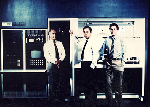
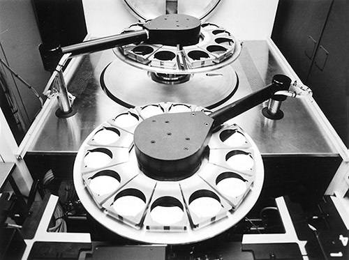
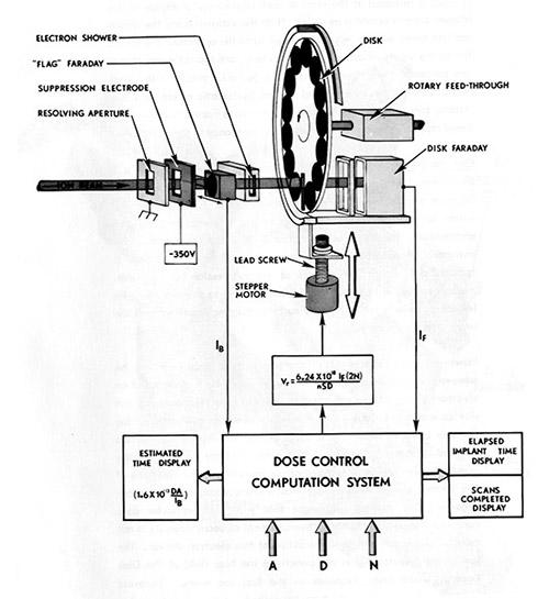
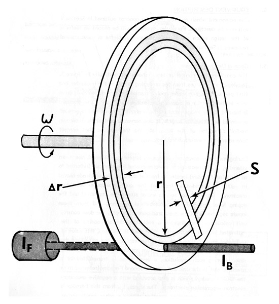
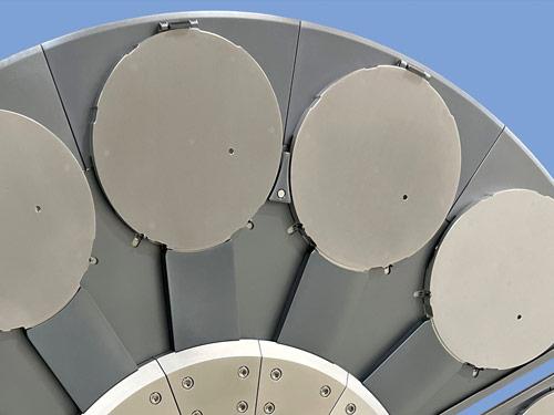
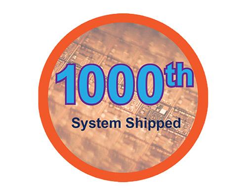
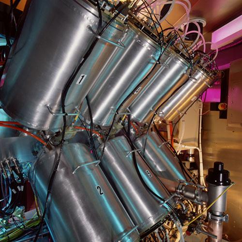
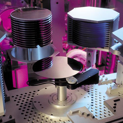
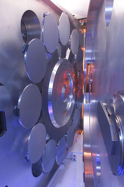
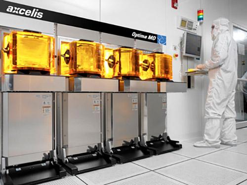
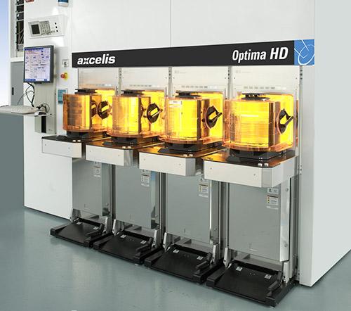
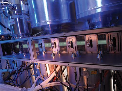
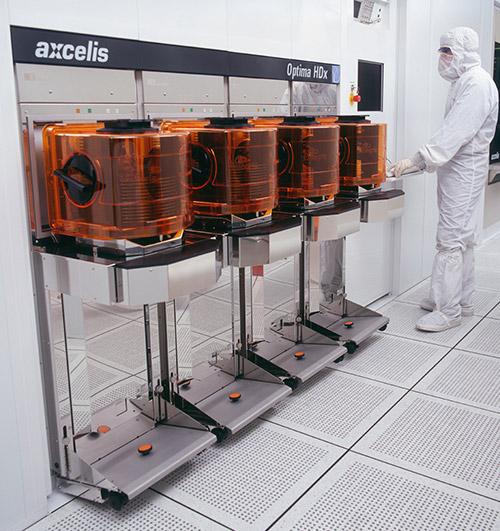
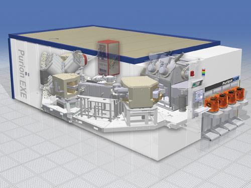
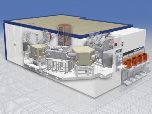
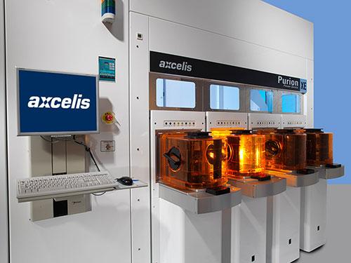
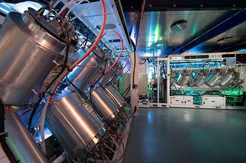
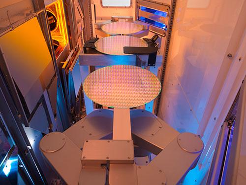
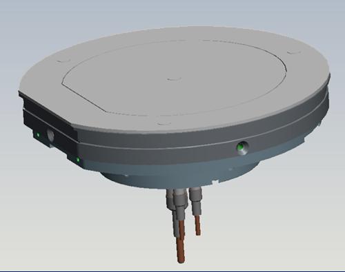
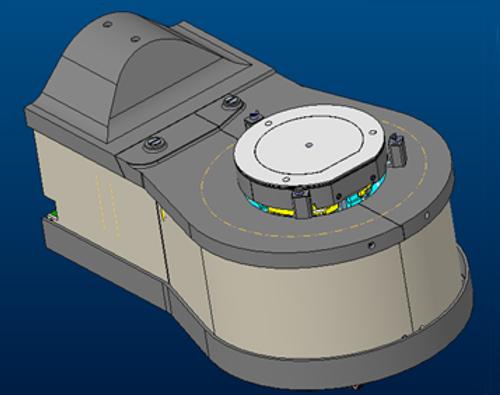
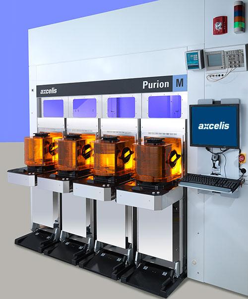
The introduction of the modern DRAM cell and the microprocessor in 1968 and 1971, respectively created a dramatic change in the electronics industry. In 1978 Nova Associates (later acquired by Eaton and spun off as Axcelis) was founded with the goal of producing the world’s first high current production implantation system. Since that fateful day, Axcelis has led the industry in ion implantation technology with an unmatched rate of new system introductions and breadth of product line. Below are some of the benchmarks of these momentous years.

The Seventies

1978
  • Nova is founded in a shed (that was a former chicken hatchery) in Middleton, MA by Geoff Ryding, Peter Rose, Andrew Wittkower and George Swanson
  • Nova receives funding from Cutler Hammer
  • NV-10 Design starts in September 1978
  • Eaton acquires Cutler Hammer and Kasper in Austin Texas, forming Eaton Semiconductor Equipment Operations
1979
  • Nova ships the first NV-10-60 from its latest facility, an abandoned bowling alley. The NV-10-60 is the industry’s first commercial high current implanter. Revolutionary design features include sliding seal technology, bi-directional mechanical scanning, superb dose uniformity, cooled disks, simple operation.

    The system featured:

    Exchange Arms
    Two disks and automated exchange arms allowed for higher throughput, though wafers were still hand loaded onto the disks

    Dose Controller
    Use of a dosimetry slot in the disk allowed for real time dose control, the velocity was proportional to 1/R

    Slot Disk
    This basic concept was carried forward successfully for many generations of NV-10, GSD, HE, HE3, HC3, Ultra, and Paradigm

  • Geoff Riding receives SEMI award for design of NV-10

The Eighties

1981
1983
  • A milestone year for the young company, Nova shipped its 100th system
  • Datalock introduced, first computer controlled supervision, another industry first
  • AT4 introduced, automating the wafer loading process
  • NV-10-160 introduced, and the single charged energy went from 80keV to 160keV
1984
  • NV-10-40 introduced
  • NV-6200 introduced
  • Banner year with record number of shipments and five separate facilities (included converted hockey rink) with shuttle service connecting the sites
1985
  • Eaton moves to its present location at 108 Cherry Hill Drive, previously the site of Cherry Hill Dairy Farm
  • The stage was set for a major transition in technology when we shipped the world’s first 200mm implanter to IBM (NV4)
  • NV-20 high current system is introduced. The system featured two Unimation Puma six axis robotic arms, which David Letterman famously used in an episode to handle viewer mail
1986
  • The NV-1000 was introduced bringing LINAC based acceleration to commercial semiconductor manufacturing. This technology would skyrocket nine years later
  • The NV-200 Oxygen implanter was introduced, ushering in an age of commercial SOI production
1988
  • NV-20A introduced with UNIX based distributed control system, an innovative approach that would span several generations of implanters
1989
  • 500th high current system ships

The Nineties

1990
  • NV-GSD is introduced and would go on to become the most successful high current implanter in the history of the industry with >600 units shipped in total, most of which are still in production. Featured unique Gyroscopic end station, the industry’s first two-axis tilt capability, for advanced processes and throughput of >200wph
  • NV-1002 high energy system introduced
  • NV-6200AV is introduced, with innovative platen design, rotation during processing and multiple tilt angles from 0 to 60 degrees
1991
  • First in industry to offer in situ particle control monitor and in situ charge monitor in a high current system as a standard feature
1993
  • Eaton Ships 1000th system
  • NV-8200P introduced featuring unmatched beam purity
  • NV-GSD/200 introduced designed for low energy performance, quick species change and high beam utilization
1994
  • Eaton introduced the world’s first production high energy system, with a throughput of 210 wph and a footprint that fits into a standard fab bay
  • The NV-GSD-HE was the integration of the GSD end station and the LINAC technology from the NV-1000 and NV-1002. This marked the beginning of another period of rapid growth and innovation
  • The growth in high energy over the next several years was extremely rapid as high energy well isolation techniques became commonplace at reasonable CoO thanks to the reliability of the LINAC design
  • The flexibility and reliability of the basic LINAC design continues to support Axcelis market leadership in high energy ion implantation
1996
  • GSD/200E2 introduced. This is still being sold today as the GSD Ovation, which was relaunched in 2021
  • One of the bigger process challenges in this era was charge control, as the gate oxide thickness was such that it was very sensitive to charge breakdown. As a result, Eaton introduced the back biased Secondary Electron Flood (SEF) to provide charge control with low risk of emitting high energy primary electrons
  • 8200P mid current implanter introduced, featuring innovative parallel scanning beam
1998
  • Introduced new 300mm implant product suite. including the MC3 for medium current, the ULE3 for ultra-low energy and the HE3 for high energy applications
  • HE3 Ships to first 300mm fab
  • Implanter Network Options introduced, the industry’s first program to provide a state-of-the-art, cost-effective method of remotely monitoring and operating ion implantation equipment –precursor to remote diagnostics systems.

The Two Thousands

2000
  • Eaton SEO is now Axcelis Technologies. Eaton corporation files registration statement to spin off Semiconductor Equipment Division, as Axcelis Technologies, Inc, in an IPO.  Eaton completes total spin off of Axcelis Technologies in December.
  • NV-8250HT Introduced, high-tilt, medium-current ion implanter introduced, designed for 0.18µm and below processes
2001
  • Eterna ELS Ion Source is introduced. Improved design promises extended source life, low cost of operation and high reliability for Axcelis ion implanters
  • Axcelis ships 1000th GSD endstation; Industry standard for proven wafer-handling reliability, productivity
  • Axcelis Technologies launches IntegraNET™ data integration and management platform; Provides framework for e-diagnostics and advanced process control
  • Axcelis introduces HC3 high current implanter for 300mm manufacturing, completing the 300mm implant product family and meeting all implant application requirements beyond 100 nanometers
2002
  • Axcelis opens $31 million advanced technology center. The 140,000-square-foot facility is dedicated to semiconductor manufacturing process development, equipment demonstration and customer training
  • Axcelis strengthens commitment to China; Opens customer service and support center in Shanghai
  • Axcelis extends reach into China’s semiconductor industry with acquisition of Tritek International
2005
  • Optima Family introduced, with launch of Optima MD medium current implanter
2006
  • Optima HD introduced, designed to address traditional high dose implants as well as the expanding range of applications in sub-65nm generation device manufacturing
2007
  • Optima XE Introduced and becomes the technology leader in single wafer high energy ion implantation
2009
  • Optima HDx high dose implanter introduced, which brings unprecedented beam current and performance levels to the high dose space

The Tens

2010
  • Optima XEx introduced, the next evolution of high energy systems
2012
  • With shipment of Purion M, the Purion Platform is born… and set a new foundation for Axcelis product development
2013
  • Purion XE introduced, featuring a 12-stage LINAC with energies up to 4.5 MeV
2014
  • Purion H introduced, featuring a unique scanned-spot-beam architecture and five filter beamline design
2016
  • Purion M SiC introduced
  • Purion EXE introduced featuring a 12-stage LINAC with energies up to 5.25 MeV
2017
  • Purion H 80 introduced, extending the energy range of a conventional high current implanter
  • Purion VXE introduced featuring a 14-stage LINAC with extended multiple charge capabilities, delivering energies up to 8 MeV
2018
  • Purion Power Series introduced, with unique features and process control capabilities, including the platform’s silicon, thin silicon and silicon carbide capability, which are enabling for the power device market
2019
  • Purion XEmax introduced, designed for emerging, high performance image sensor applications. Features dual LINAC design with patented Boost Technology™ for the highest energies up to 15 MeV
  • Purion Dragon introduced, designed for leading-edge applications, especially in low energy high dose
  • Purion H200 introduced, offering high energy, high current capability targeting the power device market

The Twenties

2020
  • Purion XE and Purion VXE Power Series introduced, designed for aluminum implantation for high volume power devices. They feature either 150mm SiC wafer handling or 200mm thin Si wafer handling
2021
  • Purion EXE Power Series SiC and Purion H200 Power Series SiC introduced. These include mechanical clamp technology for up to 650°C implant temperatures, active pre-heat, and active post cool stations
  • GSD Ovation introduced, extending the GSD series platform’s production into the future
2022
  • Axcelis Asia Operations Center opens in South Korea. The new clean manufacturing facility is designed to add capacity and drive customer satisfaction for Asia Pacific customers
2023
  • 500th Purion ships. The Purion platform is now capable of 18 configurations across 9 product backbones.
  • 45th anniversary of the company’s founding
  • The Axcelis Logistics Center opens in Beverly, MA.  The 95,600 square foot center is designed to optimize Axcelis’ warehouse and logistics operations and provide flex capacity for our manufacturing operations